Atomic Resolution Electronic Structure Scanning Transmission Electron Microscope
Atomic Resolution Electronic Structure Scanning Transmission Electron Microscope Leading-edge Equipment Home
Equipment Introduction
This Mono Cs STEM is equipped with the latest 5th order aberration corrector and monochromator, so it is possible to perform “atomic-level structure analysis (STEM), and electronic structure analysis (EELS)”. The application reaserch field is the atomic resolution studying for semiconductor, oxides, nanomaterials, and various basic science and convergence science fields.
Characteristics of the Equipment
- STEM image resolution is about < 0.08 nm at 200kV (mono off) with Cs-corrector.
- Monochromator makes energy resolution of electron energy loss spectroscopy about 36 meV (@200kV).
- Double SDD EDX system gives much higher efficiency for chemical analysis.
Representative Research Case
Local electronic structure studying of ZnO Nano particles by mono-EELS.
- STEM and EELS data for individual ZnO Nano-Particles. Red and blue arrows indicate the EELS acquisition points for surface and core regions in each NP. Comparison of the O K edge spectra obtained from the two regions, viz., surface (red) and core (blue), of each NP. Scale bars are 20 nm.
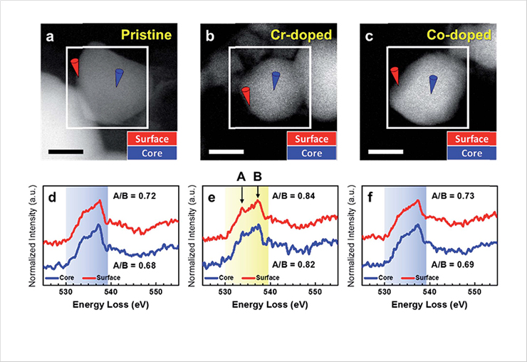 Journal of Materials Chemistry A 2020, 8, 25345–25354