Advanced in situ Surface Analysis System
Advanced in situ Surface Analysis System Leading-edge Equipment Home
Equipment Introduction
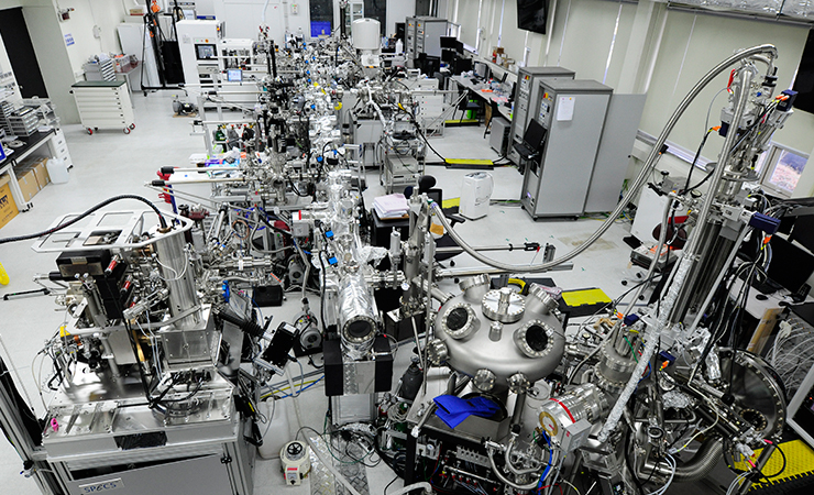
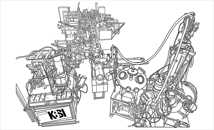
This system provides the total analytical solution to academic and industry uses by means of establishing the one-line in situ analytical system that consists of high-ends leading 7 analytical instruments and 8 device fabrication systems.
Characteristics of the Equipment
- Nanomaterial properties of metal-ceramics-semiconductor manufactured in the processing device (component, structure, form and electrical/chemical characteristics) are analyzed without the sample being exposed to air
- An analysis system was developed on a real-time basis with automatic processing devices based on the design
- The electrical/chemical characteristics can be determined under operando conditions; it is possible to manufacture the devices without being exposed to air
Representative Research Case
Study on layer-controlled MoS2 growth mechanism of Roll-to-Roll production
We developed a facile methodology for the large-scale production of layer-controlled MoS2 layers with excellent long-range uniformity and optimum stoichiometry. The capability of the MoS2 for practical applications in electronic/optoelectronic devices and catalyst for hydrogen evolution reaction is verified.
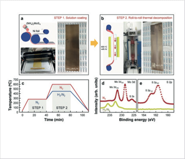 Schematic illustration and photograph of R2R production system and XPS spectra
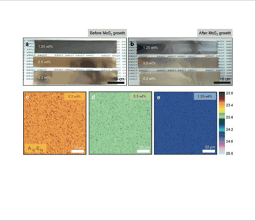 Photograph and Raman mapping images of MoS2
Application
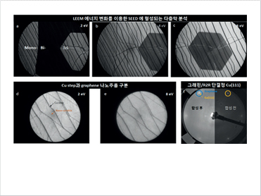 Large-scale graphene analysis platform
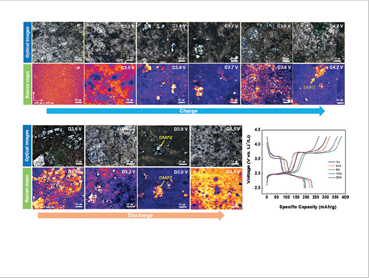 Analysis platform for Li-ion battery
Representative Research Papers
-
Catalytic Synergy on PtNi Bimetal Catalysts Driven by Interfacial Intermediate Structures
T.-S. Kim, J. Kim, H.C. Song, D. Kim, B. Jeong, J. Lee, J.W. Shin, R. Ryoo, J.Y. Park
ACS Catal. 10 (2020) 10459–10467. DOI: 10.1021/acscatal.0c02467. -
In situ work-function measurement during chemical transformation of MoS2 to MoO3 by ambient-pressure x-ray photoelectron spectroscopy
D. Lee, J. Hyuck Jang, W. Song, J. Moon, Y. Kim, J. Lee, B. Jeong, S. Park,
2D Mater. 7 (2020) 025014. DOI: 10.1088/2053-1583/ab6780. -
High-Efficiency Solution-Processed Inorganic Metal Halide Perovskite Light-Emitting Diodes
H.C.Cho, C.Wolf, J.S.Kim, H.J.Yun, J.S.Bae, H.Kim, J.-M.Heo
S.ahn, T.-W.Lee. Adv. Mater. 2017. 1700597. DOI: 10.1002/adma.201700579 -
Triangular black phosphorus atomic layers by liquid exfoliation
S.Seo, H.U.Lee, S.C.Lee, Y.S.Kim, H.Kim, J.Bang, J.H.Won, Y.Kim
B.Park. J.Lee. Sci. Rep. 2016. 6. 23736. DOI: 10.1038/srep23736 -
Strain relaxation of graphene layers by Cu surface roughening
J.H.Kang, J.Moon, D.J.Kim, Y.Kim, I.Jo, C.Jeon, J.Lee
B.H.Hong. Nano. Lett. 2016. 16. 5993-5998. DOI : 10.1021/acs.nanolett.6b01578 -
Stable semiconductor black phosphorous (BP)@titanium dioxide (TiO2) hybrid photocatalysts
H.U.Lee, S.C.Lee, J.H.Won, B.-C.Son, S.Choi. Y.Kim, S.Y.Park, H.-S.Kim, Y.-C.Lee
J.Lee. Sci. Rep. 2015. 5. 8691. doi:10.1038/srep08691 -
Formation of Frustrated Lewis Paris in Ptx-Loaded Zeolite NaY
H.Lee, Y.N.Choi, D.-W.Kim, M.Rahman, Y.I.Kim, I.H.Cho, H.W.Kang, J.-H.Seo, C.Jeon
K.B.Yoon. Angewandte. Chemie. 2015. 127. 13272-13276. DOI : 10.1002/anie.201506790. -
One-Step Synthesis of N-doped Graphene Quantum Sheets from Monolayer Graphene by Nitrogen Plasma
J.Moon, J.An, U.Sim, S.-P.Cho, J.H.Kang, C.Chung, J.-H.Seo, J.Lee, K.T.Nam
B.H.Hong. Adv. Mater. 2014. Vol(26). 3501-3505 DOI: 10.1002/adma.201306287 -
Photoluminescent carbon nanotags from harmful cyanobacteria for drug delivery and imaging in cancer cells
H.U.Lee, S.Y.Park, E.S.Park, B.Son, S.C.Lee, J.W.Lee, Y.-C.Lee, K.S.Kang, M.I.Kim, Y.G.Park. S.Choi, Y.S.Huh, S.-Y.Lee, K.-B.Lee, Y.-K.Oh, J.Lee Sci.
Rep. 2014. 4. 4665 DOI : 10.1038/srep04665 -
Innovative three-dimensional (3D) eco-TiO2 photocatalysts for practical environmental and bio-medical applications
H.U.Lee, S.C.Lee, Y.-C.Lee, B.Son, S.Y.Park, J.W.Lee, Y.-K.Oh. Y.Kim, S.Choi. Y.-S.Lee, J.Lee. Sci.
Rep. 2014. 4. 6740 doi:10.1038/srep06740 -
Rotated domains in chemical vapor deposition-grown monolayer graphene on Cu(111):an angle-resolved phtoemission study
C.Jeon, H.-N.Hwang, W.-G.Lee, Y.G.Jung, K.S.Kim, C.-Y.Park, C.-C.Hwang.
Nanoscale. 2013. Vol(5). 8210-8214. DOI: 10.1039/C3NR01700A -
N-doped Monolayer Graphene Catalyst on Silicon Photocathode for Hydrogen Production
U.Sim, T.-Y.Yang, J.Moon, J.An, J.Hwang, J.-Y.Seo, J.Lee, K.Y.Kim, J.Lee, S.Han, B.H.Hong, K.T.Nam.
Energy Environ. Sci. (2013). Vol(6). 3658-3664. DOI : 10.1039/C3EE42106F