Representative Research Publications
2017 > Representative Research Publications > Research Results Home
Development of flexible electronic device becomes possible
- Nature Communications / 2017 February
- Kim, Jong Pil (corresponding author)
Recently, development of freely deformable electronic devices is required. In this study, it is expected that freely deformable current collectors that can replace existing current collectors(rigid current collectors) have been developed and that the development of freely deformable electronic devices will be accelerated in the future.
The research team manufactured the freely deformable current collectors which plays an important role in freely deformable electronic devices. The freely deformable current collector of PET films was fabricated by using adhesive organic network film with microstructure holes. Then, a freely deformable current collector is manufactured by electroless plating of conductive metal(Cu).
In contrst to conventional PET films(Cu/PET), thin films using microstructured organic network films(Cu/MONF/PET) exhibit excellent electrical properties as a result of repeated bending tests (>1000).
The PET thin films utilizing researcher's fine structure organic network film(Cu/MONF/PET) already confirmed the possibility as the whole freely deformable current collector. In subsequent research, we are advancing the possibility of applying free deformation wearable energy storage device(lithium secon battery).
Expected Effects
The result of this research is expected to accelerate the development of flexible electronic devices expected in the forth industry, miniaturization and weight reduction of the large capacity secondary battery. And the technology utilizing microstructural junction organic network film(MONF) is expected to be utilized in various functional parts.
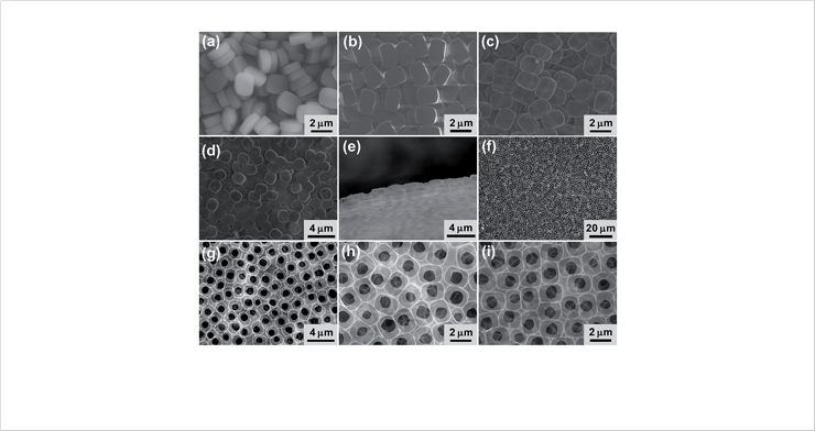 Figure. 1 SEM images of (a) the shape-controlled silica zeolite (S-SiO2),
(b) assembled zeolites on glass, (c and d) top,
Figure. 1 SEM images of (a) the shape-controlled silica zeolite (S-SiO2),
(b) assembled zeolites on glass, (c and d) top,
(e) side, (f-i) bottom view of the MONF.
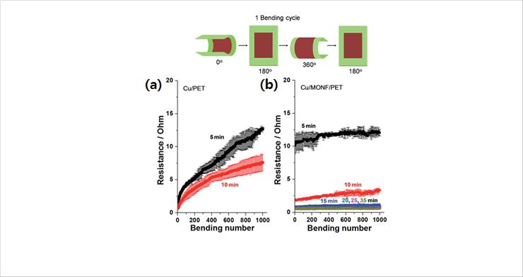 Figure. 2 (a) Bending angle dependent conductivity retention of electroless deposited
Cu/PET and Cu/MONF/PET against the repeted bending tests.