Representative Research Publications
Investigation of 2-D van der Waals Vertical Heterostructures Integrated on Deformable Substrates 2017 > Representative Research Publications > Research Results Home
Centimeter-Scale 2-D van der Waals Vertical Heterostructures Integrated on Deformable Substrates Enabled by Gold Sacrificial Layer-Assisted Growth
- Nano Letters (2017. 10.)
- Equipments : Cs-corrected STEM
Authors
Islam MA (1st author, UCF), Kim JH (SNU), Schropp A (UCF), Kalita H (UCF), Choudhary N (UCF), Weitzman D (UCF), Khondaker SI (UCF), Oh KH (SNU), Roy T (UCF), Jung Y (UCF)
Abstract
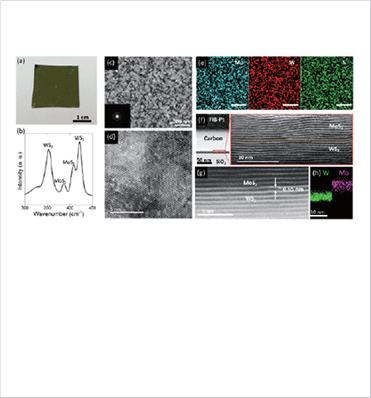
Two-dimensional (2-D) heterostructure layers assembled from vertically-stacked 2-D transition metal dichalcogenides (TMDs) exhibit large in-plane strain limits and unusual optical/electrical properties, offering unprecedented opportunities for emerging electronics and optoelectronics in new form factors. For them to be technologically viable building blocks for such unconventional technologies, it is critical to grow and integrate them onto flexible or arbitrary-shaped substrates on a large scale, which is demanded by current microelectronics manufacturing processes. We report a novel strategy to combine universally the centimeter-scale growth of 2-D heterostructure layers composed of two distinct TMDs and their direct assembly on unconventional substrates enabled by their deterministic transfer and integration. By taking advantage of the water-assisted debonding of Au interfaced with silicon dioxide (SiO2), we demonstrate the direct growth of 2-D heterostructure layers on SiO2/Au-based substrates over an area of >2 x 2 cm2 and their facile transfer and integration compatible with flexible substrates.
Expected Contribution to Science & Technology
This study opens a pathway to explore 2-D heterostructure layers as novel buiding blocks for large-scale, emerging devices of unconventional forms.
 Schematic illustration of TMDC thin film
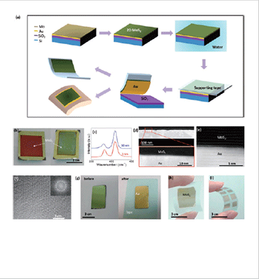 Transferred TMDC and devices test